Difference between revisions of "Component layout on PCB"
| Line 2: | Line 2: | ||
Select '''Read Netlist''' from Upper Toolbar. Click on '''Read Current Netlist'''. | Select '''Read Netlist''' from Upper Toolbar. Click on '''Read Current Netlist'''. | ||
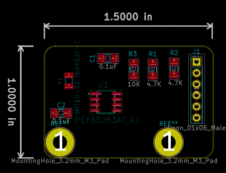
Click on components and move to place on board to match in picture. | Click on components and move to place on board to match in picture. | ||
| − | [[File: | + | [[File:PCBlayout.PNG |450px ]] |
| − | |||
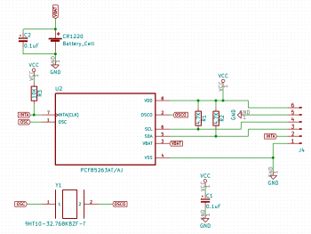
[[File:PCF85263AT-RTC.PNG |350px|mid]] | [[File:PCF85263AT-RTC.PNG |350px|mid]] | ||

