Component layout on PCB
Reading Netlist and placing footprints from components
Select Read Netlist from Upper Toolbar. Click on Read Current Netlist. Then select Close
Placing components on PCB
Click on component to select it and use the M key to move and the R key to rotate.
Place all components on board to match in picture.

Ensure the 6 Pin connector is Vertical and placed on the right side of the board.
Ensure Pin 6 VCC  on the 6 Pin connector is at the top of the board.
Ensure Pin 1 on all the Resistors are on top and are aligned with the Pin 6 VCC on the 6 Pin connector.
Ensure Pin 1 on C1 Capacitor is aligned with Pin 1 of the Resistors.
Ensure Pin 1 on Y1 Crystal is on the top.
Complete the Schematic Connecting the components in the schematic
Connecting Traces
Reading Netlist and placing footprints from components
Select Read Netlist from Upper Toolbar. Click on Read Current Netlist. Then select Close
Adjust any component that needs to be aligned.
Click on component to select it and use the M key to move and the R key to rotate.
Place all components on board to match in picture.

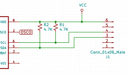
Start Routing Traces
Select Route Trace right side tool bar. Click on Pin 6 VCC and drag straight across to R2, R1 and R3.
Connect R3 to the optional C1 and to Pin 8 on the RTC

Place just above the wire as seen in picture below
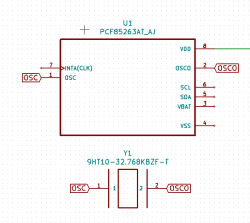
Connecting the Clock Crystal
Select Global Label right side tool bar and type OSCO in the text field.
Rotate and connect to Pin 2 of RTC.
Hover over label and hit C key to Copy the label and then connect the copy to Pin 2 of the Crystal.
Select Global Label and type OSC in the text field. Rotate and connect to Pin 1 of RTC.
Hover over label and hit C key to Copy the label and then connect the copy to Pin 1 of the Crystal.
As seen in picture below

Connecting I2C SDA & SCL
Select Place Wire from right side tool bar.
Draw a wire from the Pin 4 of the 6 Pin Connector to SCL Pin 6 of the RTC
Draw a wire from the Pin 3 of the 6 Pin Connector to SDA Pin 5 of the RTC
Draw a wire from the bottom R1 and connect to the wire running from Pin 4 to PIN 6 (SCL) of the RTC
Draw a wire from the bottom R2 and connect to the wire running from Pin 3 to PIN 5 (SDA) of the RTC
As seen in picture below

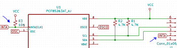
Connecting the INTA
Select Global Label right side tool bar and type INTA in the text field.
Rotate and connect to Pin 2 of the 6 Pin Connector.
Hover over label and hit C key to Copy the label and then connect the copy to Pin 7 of the RTC.
Select and Move R3 to connect bottom between the new label INTA and Pin 7 on the RTC.
Hover over the VCC symbol and hit C key to Copy the VCC symbol and then connect the VCC symbol to the
top of R3
As seen in Figure below.

Finishing up and adding the Ground
Complete the Schematic Connecting the components in the schematic
