Difference between revisions of "Component layout on PCB"
| Line 1: | Line 1: | ||
'''Reading Netlist and placing footprints from components''' | '''Reading Netlist and placing footprints from components''' | ||
Select '''Read Netlist''' from Upper Toolbar. Click on '''Read Current Netlist'''. | Select '''Read Netlist''' from Upper Toolbar. Click on '''Read Current Netlist'''. | ||
| + | '''Placing components on PCB''' | ||
Click on component to select it and use the '''M''' key to move and the '''R''' key to rotate. | Click on component to select it and use the '''M''' key to move and the '''R''' key to rotate. | ||
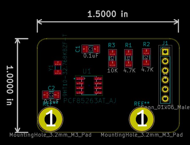
Place all components on board to match in picture. | Place all components on board to match in picture. | ||
[[File:PCBlayout.PNG |650px ]] | [[File:PCBlayout.PNG |650px ]] | ||
| + | |||
| + | '''Connecting the components in the schematic''' | ||
| + | |||
| + | |||
| + | |||
| + | |||
| + | ---- | ||
| + | ==[[ KiCad 5.0 ]]== | ||
Revision as of 19:15, 28 May 2019
Reading Netlist and placing footprints from components
Select Read Netlist from Upper Toolbar. Click on Read Current Netlist.
Placing components on PCB
Click on component to select it and use the M key to move and the R key to rotate.
Place all components on board to match in picture.
Connecting the components in the schematic
