Creating a component for KiCad Using SnapEDA
Creating a Symbol and Footprint using SnapEDA
Create a new folder in your Kicad Project folders called SnapEDA-Library
SnapEDA URL: https://www.snapeda.com/
Login or Sign up for an Account (optional)
Search Part PCF85263
Select PCF85263AT/AJ


Download Symbol and Footprint to KiCad SnapEDA Folder

1.  Click on Download Symbol and Footprint.
2.  Choose Download Format : KiCad
3.  Open Download folder and move ZIP file to KiCad SnapEDA-Library Folder
4.  UnZip the file in that folder. Move Zip file to the new folder it created or just delete it.
Or you can download the file from here PPCF85263AT RTC Symbol & Footprint
Import Symbol into KiCad
1. Open Schematic Layout Editor
2. Select Preferences from Upper Menu bar
3. Select Manage Symbol Libraries from drop down
4. Click Global Libraries tab unless you want to save this just for this project then select Project Specific Libraries .
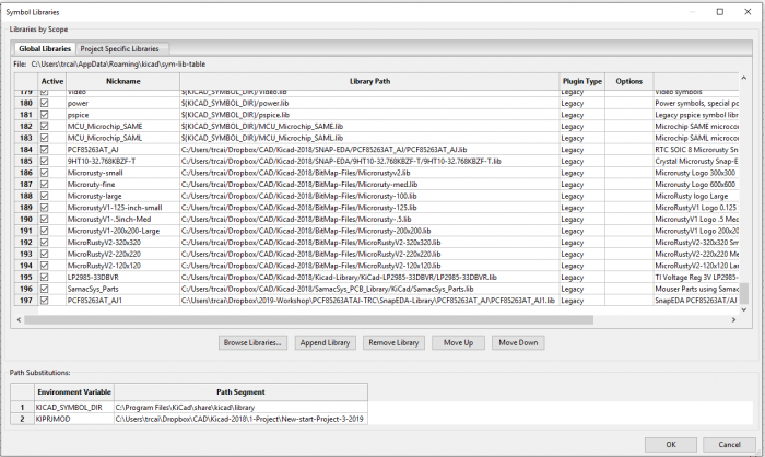
5. Click on Browse Libraries
6. Find the SnapEDA-Library folder - open that folder and find the file PCF85263AT_AJ.lib Select the file PCF85263AT_AJ.lib
7. Now add descriptions SnapEDA PCF85263AT/AJ for DMS Workshop then Click OK
 8. Select Place Symbol from Right tool bar
9. Click Mouse on Grid (Symbols Libraries will load)
10. Type in Search Field PCF85263 Select PCF85263AT/AJ then click OK
11. Place in Sector B1 Hit ESC Key.
12. Select Annotate Icon from Upper Toolbar. Click on Annotate tab.
8. Select Place Symbol from Right tool bar
9. Click Mouse on Grid (Symbols Libraries will load)
10. Type in Search Field PCF85263 Select PCF85263AT/AJ then click OK
11. Place in Sector B1 Hit ESC Key.
12. Select Annotate Icon from Upper Toolbar. Click on Annotate tab.

Import Footprint into KiCad
1.  Open PCB Layout Editor
2.  Select Preferences from Upper Menu bar
3.  Select Manage Footprint Libraries from drop down
4.  Click Global Libraries tab unless you want to save this just for this project then select Project Specific Libraries .
5.  Click on Browse Libraries
10. Find the SnapEDA-Library folder - open that folder and find the file PCF85263AT_AJ.mod Select the file PCF85263AT_AJ.mod
11. Now add descriptions SnapEDA PCF85263AT/AJ for DMS Workshop. Click OK
12. Open Schematic Layout Editor
13. Select Assign PCB Footprint to Schematic Symbol Icon from Upper Toolbar.
14. After Footprints loads select from center column PCF85263AT_AJ then select from Left Column PCF85263AT_AJ
    Select Line item 1 PCF85263AT/AJ:SOIC127P600X175
15. Select Generate Netlist from the Upper Toolbar. Click on Generate Netlist - Save File
16. Open PCB Layout Editor
16. Select Read Netlist from Upper Toolbar. Click on Read Current Netlist. Click on components and move to place on board.
Add the Crystal 9HT10-32.768KBZF-T
1. Search for 9HT10-32.768KBZF-T in the Snap EDA search.
2. Follow the same steps that are used to download the PCF85263 RTC
3. Download 3D Model and place in the SnapEDA folder.
Or you can download the files from here:
RTC PPCF85263AT Symbol & Footprint
Crystal 9HT10-32.768KBZF Symbol, Footprint & 3D Model
Let's finish the project drawing
Complete the Schematic Layout